G4-Scope
This is an exploration into the combination of analog and digital "computing". The aim is to show electrical signals as graph on a screen, i.e. to implement an oscilloscope. The first constraint is that it must fit on a 7x3 or 7x5 cm PCB so that it can be turned into a module later. The second constraint is that it must be doable for me :) - I don't have any formal electronics design training. That's really the point of this: to learn how a "scope" works.
Hardware
A STM32G431CB µC is used as the brains: its two ADCs can sample at up to ≈ 5 Ms/s, the CPU clock goes up to 170 MHz, it has 32 KB RAM, and there's 128 KB of flash memory. There's enough here for an extensive exploration and implementation.
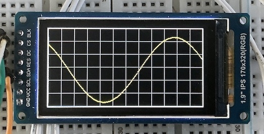
The display is a small 1.9" 320x170 pixel display. Just enough to display a "graticule" area with 12 divisions across and 6 divisions vertically.
The G4-Scope is controlled by buttons and one or two rotary encoders, but these will need to be on a separate module. There's no way to fit these on one PCB with the display.
For development, a Black Magic Probe is used, using an STM32F411 "Black Pill" board.
That, plus a breadboard and some wires, is about it. The total cost with parts from AliExpress was no more than about €30, as of mid-2026.
Once the basic design and build works, an analog front end of some kind will need to be added. But that's a bit further down the road ...
Software
On the software side, it's all based on PlatformIO and JeeH. I'm developing this on MacOS, but Linux and Windows should work equally well. See JeeH's getting started for details.
All software development is based on the source code in this area: https://codeberg.org/jcw/dobb/src/branch/main/apps/g4-scope/.
Built-in peripherals
There are a lot of moving parts in this project. From figuring out a "good" development cycle to implementing and debugging the many different hardware details for high-speed signal acquisition and visualisation. The G4-Scope is bound to be a pretty long adventure ...
Blinking LED
The first build verifies that the G431 has power and is properly connected to the Black Magic Probe (BMP), and that the LED blinks once compiled and uploaded. It's based on this code:
blink.cpp
The command to build and upload is:
Console output via RTT
See the JeeH info about RTT for details. This needs a serial connection to the BMP to display messages. That connection can then be kept open across all uploads: very convenient!
console.cpp
Sample output on the debug console, i.e. the BMP's serial USB port:
Note
This same source code structure will be used in all the following "gradual enhacement" examples.
DAC + ADC check
Next step: read out the ADC. The built-in DAC can feed different input voltages as a first test. It looks like in analog mode mode ADC and DAC can be inter-connected on one pin:
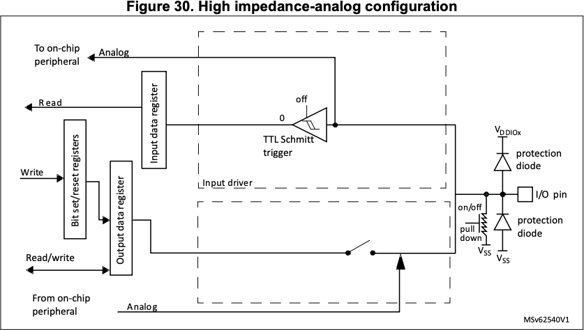
Unfortunatelt, JeeH's built-in ADC driver is not quite up to it. It's a simple implementation for ADC1, not for ADC2 (connected to DAC1's output). So for now, I'll jumper A4 to A1.
dac2adc.cpp
#include <jee.h>
#include <jee/hal.h>
using namespace jeeh;
#include "defs.hpp"

int main () {
    initBoard();

    Pin::config("A4:A");
    dac::init(); // currently hard-coded for DAC1, output pin A4
    adc::init(); // currently hard-coded for ADC1
    msWait(2); // TODO needs > 1 ms settling time, but why?

    // this code needs a jumper between DAC out (A4) and ADC in (A1)

    const uint16_t steps [] = {
        0, 1000, 2000, 3000, 4000, 4095, 4000, 3000, 2000, 1000, 0,
    };

    for (auto e : steps) {
        dac::set(e);
        msWait(1);

        logf("%4d => %4d %4d %4d", e,
            adc::read(2), adc::read(2), adc::read(2)); // A1 is ADC1 channel 2
    }

    while (true) { led.toggle(); msWait(500); }
}
Sample output, with different DAC values and three quick ADC conversions:
dac2adc: STM32G431xx @ 170 MHz (v7.0.9-13-gc89bf101)
   0 =>   11    0    0
1000 =>  960  927  931
2000 => 2016 1977 1982
3000 => 3087 2968 2969
4000 => 3936 3936 3936
4095 => 3983 3992 3992
4000 => 3936 3936 3936
3000 => 2951 2972 2969
2000 => 1927 1982 1980
1000 =>  927  927  931
   0 =>    0    0    0
It works: the DAC voltages are converted back to digital by the ADC. The measurements are a few percent off, and it looks like the top value is never reached. The DAC buffer is probably not strong enough to drive an ADC with a minimum sample time (it needs a low-impedance input to quickly charge/discharge the sample-and-hold capacitor).
Warning
With fastClock() in defs.hpp disabled, the results are a bit different.
All ADC readings are now much closer to the expected values:
Continuous DAC output
For more tests involving the ADC, a stable signal of some kind would be useful. This can be generated with the DAC and a DMA channel in circular buffer mode to continuously feed it. A hardware timer can set the pace at which the DMA feeds new values to the DAC.
But first I need a sine wave ...
CORDIC
For the sake of using as much of the µC's built-in hardware as possible, I'm generating the sine wave using the built-in CORDIC hardware. From the reference manual:
The CORDIC coprocessor provides hardware acceleration of mathematical functions (mainly trigonometric ones) commonly used in motor control, metering, signal processing, and many other applications.
cordic.cpp
Sample output:
cordic: STM32G431xx @ 170 MHz (v7.0.9-14-g6699c955)
     0                                +
 12539                                            +
 23170                                                      +
 30273                                                             +
 32767                                                               +
 30273                                                             +
 23170                                                      +
 12539                                            +
     0                                +
-12539                    +
-23170          +
-30273   +
-32767 +
-30273   +
-23170          +
-12539                    +
     0                                +
Ok, that's a sine wave. And it's in full 16-bit resolution, more than enough for a 12-bit DAC.
Sine wave
Here's a test to drive the DAC from a sine wave table and plot the ADC readings.
It uses cordic::sineFill() to prepare a vector with sinewave values in a
specified range:
sinegen.cpp
#include <jee.h>
#include <jee/hal.h>
using namespace jeeh;
#include "defs.hpp"

int main () {
    initBoard();
    cordic::init();

    Pin::config("A4:A");
    dac::init(); // currently hard-coded for DAC1, output pin A4
    adc::init(); // currently hard-coded for ADC1
    ADC1[0x14](0,3) = 7; // max ADC sample time, to let weak DAC output settle
    msWait(2); // TODO needs > 1 ms settling time, but why?

    // this code needs a jumper between DAC out (A4) and ADC in (A1)

    uint16_t wave [20];
    cordic::sineFill(wave, 0x0100, 0x0F00); // avoid the 12-bit DAC's extremes

    for (auto e : wave) {
        dac::set(e);
        msWait(1);

        adc::read(2);          // A1 is ADC1 channel 2
        auto v = adc::read(2); // use 2nd reading, it's more accurate
        logf("%4d %4d %*c", e, v, v/64, '+');
    }

    while (true) { led.toggle(); msWait(500); }
}
Sample output:
sinegen: STM32G431xx @ 170 MHz (v7.0.9-15-g53c6c526)
2048 2016                               +
2602 2552                                       +
3101 3078                                                +
3498 3487                                                      +
3752 3743                                                          +
3840 3815                                                           +
3752 3743                                                          +
3498 3487                                                      +
3101 3079                                                +
2602 2555                                       +
2048 2031                               +
1494 1439                      +
 995  926              +
 598  536        +
 344  280    +
 256  192   +
 344  280    +
 598  527        +
 995  926              +
1494 1438                      +
As before, the ADC readings aren't 100% accurate, but I've increased the ADC's sampling time to let the DAC's weak output signal settle a bit more than before. Also, to avoid the DAC limits at the both ends of its range, only values 0x0100 .. 0x0F00 are used.
It'll have to do for now - DAC buffering and accuracy can be addressed later.
Periodic timer
To generate a signal without the CPU, a DMA channel needs to be periodically triggered to copy the next value from the sine table to the DAC. That's done with a hardware timer. This test uses TIM3, because it's also able to drive the LED on pin C6:
timer.cpp
common.h: initTimer3
void initTimer3 (uint16_t div, uint16_t cnt, uint8_t pct =50) {
    enum { CR1=0x00, CCMR1=0x18, CCER=0x20, PSC=0x28, ARR=0x2C, CCR1=0x34 };

    RCC(ena::TIM3,1) = 1;
    TIM3[CCMR1](0,8) = 0x68; // OC1PE, OC1MR: PWM mode 1
    TIM3[CCER](0) = 1;       // CC1E

    TIM3[PSC] = div - 1;
    TIM3[ARR] = cnt - 1;
    TIM3[CCR1] = (cnt*pct) / 100; // duty cycle 1..100%

    TIM3[0x0C](9) = 1;  // DIER: CC1DE to trigger DMA
    TIM3[CR1](0) = 1; // CEN
}
And sure enough, the LED blinks with a 10% duty cycle. This timer can now be re-used to drive the DMA at a much higher rate.
Info
This code is a first example of "taking over" control of built-in hardware, as JeeH does not include an API to set up and use hardware timers. There is so much variation between them, and there are so many use cases and chip families, that I saw no way to implement a generic and practical wrapper.
Then again, this is how JeeH was meant to be used in non-trivial apps: Use STM's Reference Manual !
DMA to DAC
All the parts now exist to generate a sine wave while leaving the CPU free for other tasks. Here's a first test, generating a slow slne wave which the app then verifies via the ADC:
slowsig.cpp
#include <jee.h>
#include <jee/hal.h>
using namespace jeeh;
#include "defs.hpp"
#include "common.h"

constexpr feed::Config DAC_CONF = { DAC1.ADDR+0x08, DMA1.ADDR, 1-1, 1-1, 61 };
feed::DmaFeed<DAC_CONF> feeder;

int main () {
    initBoard();
    cordic::init();

    uint16_t wave [4096];
    cordic::sineFill(wave, 0x0100, 0x0F00);

    // system clk = 170 MHz, timer clk = 10 KHz, trigger = 2 KHz, freq ≈ 0.5 Hz
    initTimer3(17'000, 5);

    Pin::config("A4:A");
    dac::init(); // currently hard-coded for DAC1
    feeder.init(wave, sizeof wave / sizeof *wave); // stream from wave[] to DAC

    adc::init(); // currently hard-coded for ADC1
    ADC1[0x14](0,3) = 7; // max ADC sample time, to let weak DAC output settle

    // this code needs a jumper between DAC out (A4) and ADC in (A1)

    for (auto i = 0; i < 20; ++i) {
        msWait(100);
        adc::read(2);          // A1 is ADC1 channel 2
        auto v = adc::read(2); // use 2nd reading, it's more accurate
        logf("%4d %*c", v, v/64, '+');
    }

    while (true) { led.toggle(); msWait(500); }
}
Sample output:
slowsig: STM32G431xx @ 170 MHz (v7.0.9-18-g07f9a5ac)
2791                                           +
3296                                                   +
3615                                                        +
3808                                                           +
3808                                                           +
3615                                                        +
3231                                                  +
2752                                           +
2183                                  +
1567                        +
1048                +
 608         +
 384      +
 192   +
 384      +
 543        +
 952              +
1510                       +
2072                                +
2672                                         +```
The sine wave table has 4096 entries to support the full resolution of the DAC: since the derivative of a sine wave is always in the range [-1,+1], a 12-bit DAC never changes by more than ±1 at a time when the wave is spread out over 4096 steps. Because the STM's DAC rate limit is one million samples per second, the full-resolution frequency output can be at most ≈ 250 Hz. For initial tests, this sine wave signal will be fine.
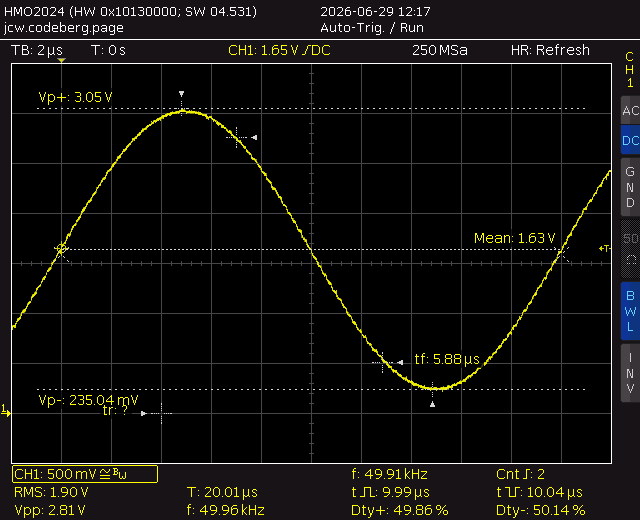
DAC at 5 Ms/s
It turns out that the DAC can in fact be driven at a higher rate than its specified 1 Ms/s limit, with excellent results. A sine wave only changes in small steps after all. Here's the 50 KHz signal when the DAC is driven at 5 Ms/s with a 100-sample sine, as captured by my trusty 200 MHz Hameg oscilloscope.
That concludes the analog part of this initial G4-Scope exploration.
Adding an LCD display
The 1.9" LCD display fits (just barely) on a 7x3 cm PCB. Its 320x170 pixel resolution is minimal but sufficient, and it turns out to be surprisingly readable at close distance.
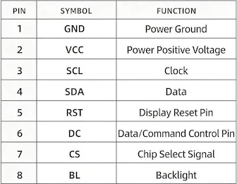
The display is connected via SPI, using a total of 6 signal and 2 power wires:
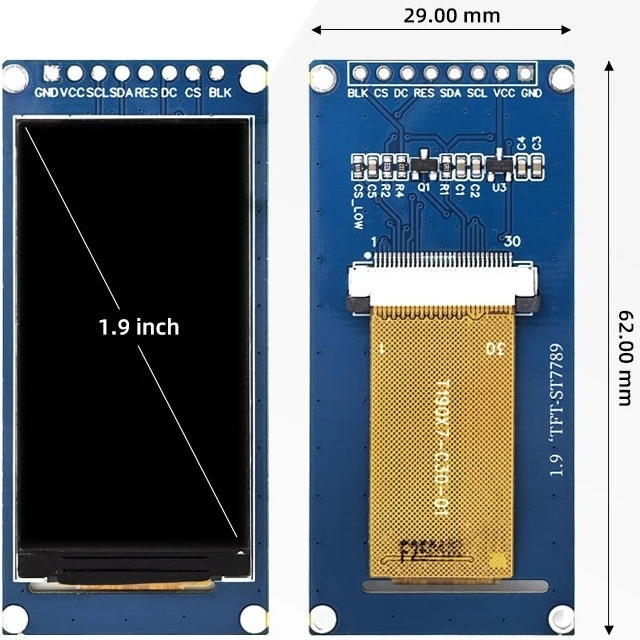
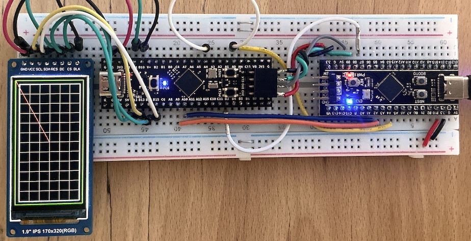
The first step is to specify all the pin connections in the platformio.ini
file:
This is turned into #define settings by JeeH's code
generator as part of the build process:
defs.hpp
// Lines with "CG" control the code-generated parts of this file.

//CG1 board leds
#define LED  "C6"

const Pin led (LED,"P");

//CG3 board pins
#define PINS_BKL "B10"
#define PINS_RST "B11"
#define PINS_DC "B14"

//CG[ board spi
#define SPI_NAME SPI2
constexpr spi::Config SPI_CONF {
    "B15:H5,B14,B13,B12:HP", SPI2.ADDR, ena::SPI2, 170,
};
//CG]

spi::Poll<SPI_CONF> spiBus; // st7789 lcd

//CG[ board uart
#define UART_NAME USART1
#define UART_TRIGGER(w) extern "C" { \
    void DMA1_Channel1_IRQHandler () { (w).irqTx(); } \
    void DMA1_Channel2_IRQHandler () { (w).irqRx(); } \
    void USART1_IRQHandler () { (w).irqIdle(); } \
}
constexpr uart::Config UART_CONF {
    "B6:O7", USART1.ADDR, ena::USART1, false, 170,
    DMA1.ADDR, 1-1, 1-1,2-1, 25,24,
    Irq::DMA1_CH1, Irq::DMA1_CH2, Irq::USART1, 64, 128,
};
//CG]

uart::Trig<UART_CONF> linBus;
UART_TRIGGER(linBus)

rtt::Desc rttDesc;

void jeeh::logWriter (const void* ptr, size_t len) {
    rttDesc.tx.write((const char*) ptr, len);
}

void initBoard () {
    fastClock();
    rttDesc.tx.flags = 2; // set RTT output to blocking mode
    cycles::init();

    logf("\n%s: %s @ %d MHz (%s)",
            PIOENV, SVDNAME, SystemCoreClock / 1'000'000, VERSION);
}
JeeH has a "TwoDee" package with a set of high-level graphics primitives. It's now simple to draw a "graticule" grid, plus a few extra lines to verify the display's size and orientation:
lcdtest.cpp
#include <jee.h>
#include <jee/hal.h>
#include <jee/dev/st7796.h>
using namespace jeeh;
#include "defs.hpp"
#include "common.h"

using Screen = dev::ST7796<LcdSpi,170,320,35>; // 1.9" LCD module
util::TwoDee<Screen> gfx;

int main () {
    initBoard();
    initGrid(gfx);

    // draw a a box of maximum size, and a line from origin to the middle
    // to verify proper setup and orientation: (0,0) should be bottom left

    gfx.fg = GREEN; gfx.box({0, 0, Screen::width-1, Screen::height-1});
    gfx.fg = RED;   gfx.line({0,0}, {Screen::width/2, Screen::height/2});

    while (true) { led.toggle(); msWait(500); }
}
common.h: initGrid
See also the image at the top of this page for a first "scope-like" impression.
Info
This code is starting to become a bit more involved, using C++ templates to tie things together. That's how "modern" C++ works: combine code in a type-safe manner without having to use virtual function calls. The main benefit is performance, as the compiler can optimise such code considerably better than runtime "vtables". When used with care, it also becomes smaller (but ... it's easy to get that wrong!).
Polled ADC capture
Now that the DAC generates a continuous sine wave, the CPU is available to show some information on the LCD display. Such as a trace captured via successive ADC reads:
adc2lcd.cpp
#include <jee.h>
#include <jee/hal.h>
#include <jee/dev/st7796.h>
using namespace jeeh;
#include "defs.hpp"
#include "common.h"

using Screen = dev::ST7796<LcdSpi,170,320,35>; // 1.9" LCD module
util::TwoDee<Screen> gfx;

constexpr feed::Config DAC_CONF = { DAC1.ADDR+0x08, DMA1.ADDR, 1-1, 1-1, 61 };
feed::DmaFeed<DAC_CONF> feeder;

int main () {
    initBoard();
    initGrid(gfx);
    cordic::init();

    uint16_t wave [4096];
    cordic::sineFill(wave, 0x0100, 0x0F00);

    // system clk = 170 MHz, timer clk = 10 MHz, trigger = 2 MHz, freq ≈ 500 Hz
    initTimer3(17, 5);

    Pin::config("A4:A");
    dac::init(); // currently hard-coded for DAC1
    feeder.init(wave, sizeof wave / sizeof *wave); // stream from wave[] to DAC

    // this code needs a jumper between DAC out (A4) and ADC in (A1)

    adc::init(); // currently hard-coded for ADC1
    for (auto x = 1; x < GW; ++x) {
        auto v = adc::read(2); // A1 is ADC1 channel 2
        uint16_t y = (v * GH) / 4095;
        gfx.pixel({TB+y, TL+x}, YELLOW);
    }

    while (true) { led.toggle(); msWait(500); }
}
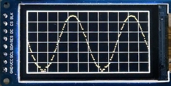
The ADC values cover slightly less than the full 12-bit range, since that's how
the sine wave table was set up. With some rescaling, this can then be shown as
pixels in the "trace area" of the LCD, which is set to 300 by 150 pixels (TW x
TH).
There are a number of glitches and artifacts in the graph shown here. As before, the DAC is struggling to properly drive the ADC. This will be addressed later.
The signal frequency was set by trial and error to capture about two full cycles: the DAC is triggered at 2 Ms/s. With a sine table of 4096 samples, that corresponds to 500 Hz = 2 ms cycle time. So the graph takes about 4 ms to capture and draw 300 samples in a loop.
That's 13.3 µs per sample, a 75 KHz sampling rate. Nice, but only good enough for audio signals. The ADC is much faster than that, but the display update is the bottleneck here.
DMA-based capture
It's time to set up a second DMA channel, which can capture ADC readings without having to use a CPU-heavy software loop. Drawing the graph still takes most of the time, but this can be done once all the data has been saved.
dma2lcd.cpp
#include <jee.h>
#include <jee/hal.h>
#include <jee/dev/st7796.h>
using namespace jeeh;
#include "defs.hpp"
#include "common.h"

using Screen = dev::ST7796<LcdSpi,170,320,35>; // 1.9" LCD module
util::TwoDee<Screen> gfx;

constexpr feed::Config DAC_CONF = { DAC1.ADDR+0x08, DMA1.ADDR, 1-1, 1-1, 61 };
feed::DmaFeed<DAC_CONF> feeder;

constexpr capt::Config ADC_CONF = { ADC1.ADDR, DMA1.ADDR, 1-1, 1-1,2-1, 5,5 };
capt::Capture<ADC_CONF> capture;

int main () {
    initBoard();
    initGrid(gfx);
    cordic::init();

    uint16_t wave [100];
    cordic::sineFill(wave, 0x0100, 0x0F00);

    // system clk = 170 MHz, timer clk = 10 MHz, trigger = 5 MHz, freq = 50 KHz
    initTimer3(17, 2);

    Pin::config("A1:A");
    capture.init(2); // pin A1 is ADC1 channel 2

    Pin::config("A4:A");
    dac::init(); // currently hard-coded for DAC1
    feeder.init(wave, sizeof wave / sizeof *wave); // stream from wave[] to DAC
    msWait(1); // let it stabilise

    // this code needs a jumper between DAC out (A4) and ADC in (A1)

    uint8_t dat [GW];
    capture.read(dat, GW);

    for (auto x = 1; x < GW; ++x) {
        uint8_t y = (dat[x] * GH) / 255;
        gfx.pixel({TB+y, TL+x}, YELLOW);
    }

    while (true) { led.toggle(); msWait(500); }
}
common.h: Capture
template< const Config& C >
struct Capture {
    enum { ISR=0x00, CR=0x08, CFGR=0x0C, SMPR1=0x14, SQR1=0x30, DR=0x40,
            CCR=0x308, CDR=0x30C };

    static constexpr dma::DmaConfig<Config,C> dma {};

    void init (uint8_t chan1, uint8_t chan2 =0) {
        auto dual = chan2 != 0;
        adc::init(dual);

        ADC1[CR](0) = 0;      // ~ADEN
        if (dual)
            ADC2[CR](0) = 0;      // ~ADEN

        ADC1[CFGR](13) = 1;   // CONT
        ADC1[CFGR](3,2) = 2;  // RES 8-bit

        if (!dual)
            ADC1[CFGR](0) = 1;    // DMAEN
        else {
            ADC2[CFGR](13) = 1;   // CONT
            ADC2[CFGR](3,2) = 2;  // RES 8-bit

            ADC1[CCR](14,2) = 3;  // MDMA 8-bit
            ADC1[CCR](8,4) = 5;   // DELAY 6 bits (total: 3.5+8+0.5)

            if (chan1 != chan2 || chan1 > 2)
                ADC1[CCR](0,5) = 6; // DUAL regular simultaneous
            else {
                // both on A0 (tied to A2), or both on A1 (w/o opamp)
                ADC1[CCR](0,5) = 7; // DUAL regular interleaved
                                    //
                // one extra sampling cycle to get even timing
                ADC1[SMPR1](31) = 1;  // SMPPLUS
                ADC2[SMPR1](31) = 1;  // SMPPLUS
            }
        }

        ADC1[CR](0) = 1;          // ADEN
        if (!dual)
            dma.init(C.base + DR, C.base + DR);
        else {
            ADC2[CR](0) = 1;      // ADEN

            dma.init(C.base + CDR, C.base + CDR);
            dma.DRX[dma::CCR](10,2) = 1; // MSIZE 16b
            dma.DRX[dma::CCR](8,2) = 1;  // PSIZE 16b
        }

        ADC1[SQR1] = chan1 << 6;
        if (dual)
            ADC2[SQR1] = chan2 << 6;
    }

    void read (uint8_t* ptr, size_t num) {
        dma.rxStart(ptr, num);
        ADC1[CR](2) = 1; // ADSTART
        while (!dma.rxCompleted()) {}
    }
};
There is no need for a timer, the DMA can trigger as soon as the ADC has a new sample, and keep doing so until the buffer is full. So the logic is now: capture 300 samples at top speed, then draw them on the display.
The ADC resolution has been reduced from 12 to 8 bits for maximum performance, as the display only uses 150 vertical pixels anyway. The ADC's clock is set to 170/3 ≈ 56.6 MHz, slightly less than its maximum of 60 Mhz. Reducing the system clock to 150 MHz would support a 60 MHz ADC clock, but then the CPU clock speed will drop from 170 to 150 MHz.
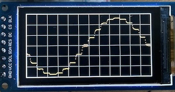
The capture rate is now dramatically higher: the sine table has only 20 items and they are sent to the DAC at 1 Ms/s, so this is a 50 KHz sine wave = 20 µs per cycle. The ADC gets 300 samples in those 20 µs ... 15 Ms/s ?
As clearly visible in this capture, the DAC needs some time to settle and can only somewhat approximate a sine wave with its 20 sine table values.
Note that it will be very simple to slow down the ADC by increasing its sampling time, adjusting its clock prescaler, and/or over-sampling to average out multiple readings.
That can't be right!
The latest result shows that the DAC generates a 50 kHz signal (verified), which takes 20 µs per cycle, and there's about one cycle on the display. The graph area is 300 pixels wide and since each pixel is one ADC sample, this implies that the ADC is sampling at ≈ 15 MHz.
But this is 3 times the maximum supported sampling rate of the STM32G4's ADC!
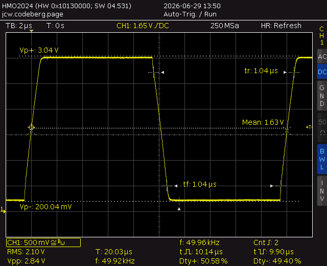
As first check, I changed the DAC signal to generate a square wave:
const auto NWAVE = 100;
uint16_t wave [NWAVE];
for (auto i = 0; i < NWAVE; ++i)
    wave[i] = i < NWAVE/2 ? 0x100 : 0xF00;
feeder.init(data, NWAVE);
This produced the square wave shown: 50 kHz, 1 µs rise and fall times, exactly as expected from the specs (even though the DAC is driven 5x faster than specified).
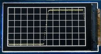
Here is the same signal sampled by the ADC and then shown on the LCD. There are 15 .. 20 dots on the rising edge, which indicates that the ADC has sampled that many times ... within one microsecond ???
Solved
The code was running on HSI (16 MHz) instead of HSE (8 MHz), because another
G431 board I use doesn't have a crystal mounted (the price of copy-and-paste
...). And the HSI code path in fastClock() had not been adjusted for the
60 MHz PLL divider for the ADC. Now everything is back to sampling at the the
expected 5.1 Ms/s rate.
Note
Quite surprising, but good to know that the G4's ADCs ran just fine at 3x their rated speed.
Analog options
The main hardware and software components are working: a DAC generates a continuous signal using DMA and the ADC acquires samples to show a trace on the LCD display. It all runs at high speed, and the CPU is only really involved in updating the display via SPI.
And yet, that's just a start: the G431 also has three built-in op-amps with programmable gain (PGA) and three more DAC channels. There's a lot of flexibility to be had with all this.
A major enhancement would be to acquire two separate signals, a.k.a. a "dual-trace" scope. A related option is to pair up those two ADCs on the same input in "interleaved" mode for twice the acquisition rate, i.e. 10 iso 5 Ms/s (single-channel only, evidently).
Another option: with a PGA op-amp + DAC you can adjust the bias point for an input signal and then amplify it to increase the input sensitivity while still using each ADC's full range. This won't replace an analog front-end but does add flexibility, and it's all part of the G431.
Signal generator
The G431 has two dual-channel DACs: DAC1 and DAC3 (there's no DAC2). DAC1 can drive external pins (with an optional weak buffer stage), whereas DAC3 can only be used by other analog hardware inside the G431. But DAC3 is much faster: it can be driven at up to 15 Ms/s, vs 1 Ms/s for DAC1.
DAC3 channel 2 can be used as input for OPAMP3, and the output of the opamp can drive an external pin, so that's what I'm going to use as "signal generator" output. This is where JeeH's built-in utility code ends: it requires taking over the hardware from application code. It's not complicated, but it relies on STM's "STM32G4 Reference Manual" (PDF: RM0440):
common.h: dac3init
void dac3init () {
    enum { CR=0x00, DHR12R1=0x08, DHR12R2=0x14, MCR=0x3C };

    RCC(ena::DAC3,1) = 1;
    DAC3[MCR](16,3) = 7;  // MODE2: internal, no buffer
    DAC3[MCR](14,2) = SystemCoreClock / 80'000'000; // HFSEL: 0, 1, or 2
    DAC3[CR](0) = 1;      // EN1
    DAC3[CR](16) = 1;     // EN2

    enum { CSR1 = 0x08 };

    RCC(ena::SYSCFG,1) = 1; // enable opamps
    OPAMP[CSR1](7) = 1;   // OPAHSM
    OPAMP[CSR1](5,2) = 3; // VM_SEL follower
    OPAMP[CSR1](2,2) = 3; // VP_SEL DAC3 CH2
    OPAMP[CSR1](0) = 1;   // OPAEN
}
The DMA destination has also been changed to DAC3's register. DAC3 is really much faster than DAC1: the rise/fall times of a square wave drops to ≈ 70 ns, a 15x improvement.
And since this DAC is driven by DMA, it turns into an Arbitrary Waveform Generator (AWG). The output on pin B1 will be one of the IO pins once this G4 scope is turned into a module.
Bias voltages
Now that DAC3 has been turned into a signal generator, this frees up DAC1. Those two independent outputs can now be used as optional BIAS voltages for OPAMP1 and OPAMP2.
Setting DAC1 is as easy as before, here's how to set two output voltages from software:
dac::init(true); // both channels
dac::set(0x0780, 0x0980); // set output voltages on A4 and A5, respectively
Pin allocations
Assigning the proper pins on a G431's 48-LQFP page is both delightful and maddening ... There are many options to choose from, but they are also very constraining: only certain pins can be used for certain functions. And some of the useful combinations can only be achieved via external wiring. But in the end, it looks like everything I wanted to be able to do is indeed feasible:
- Two analog input channels, each with its own ADC.
- Pin A1 can be used as ADC1 input, and pin A7 as ADC2 input.
- Both ADCs can be set to use pin A1 in interleaved mode.
- OPAMP1 can use A1 as "+" input, OPAMP2 can use A7 as "+".
- ADC1 can use OPAMP1's output (internally, or via A2).
- ADC2 can use OPAMP2's output (internally, or via A6).
- Pins A4 and A5 are the two settable DAC1 bias voltages, respectively.
With a wire from B1 to A0, from A4 to A3, and from A4 to B0, several more signal routing options are possible, all controlled from software.
So in the end, A1 and A7 are the ADC / OPAMP inputs, and B1 is the DAC / OPAMP output.
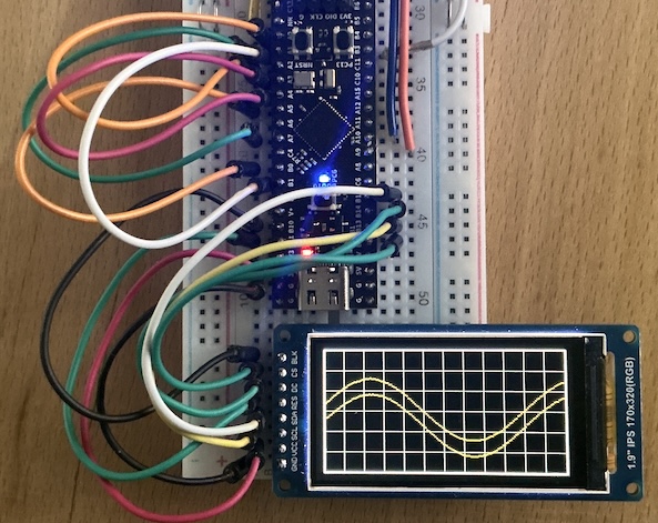
There are still many details to figure out to get all the variations working, but here's a first preview of a dual-trace capture. It routes both signals through their op-amps and amplifies them 4x before capturing each one at 5 Ms/s. DAC3 is used to generate the 40 KHz sine wave at 15 Ms/s.
The CPU is only involved in setup, signal processing, and graphics. One DMA channel drives the 12-bit DAC, and another one captures the 8-bit ADC streams (as pairs of bytes).
Who would have thought that a tiny STMG431 chip could do all of this at the same time, eh?
Op-amps
The two spare op-amps in the G431 can be used in front of ADC1 and ADC2. The main reasons for doing so is that it can be a voltage follower with a high input impedance and a stronger output signal into the ADC.
But these op-amps can also be configured with a programmabe gain from 2x to 64x. Given that the low-end of the input range is best kept slightly above GND, this can only be used in combination with an adjustable bias voltage, i.e. adjusted "ground" reference. That's where the two DAC channels come in: they can be used as reference voltage for the built-in PGA coltage divider on the "-" input pin.
The G431 allows either a follower mode without bias, or a 2..64x PGA mode with bias. This is not really a problem, since a voltage follower doesn't change the input signal: both input and output are limited to [0,3.3V], any offset can be removed after the ADC conversion. For the PGA mode, the bias level is essential to avoid hitting either "rail".
Here is the code which can set the opamps in the desired mode:
common.h: opaInit
void opaInit (uint8_t num, uint8_t gain =0) {
    // re-use the same IoReg to adjust different bit fields
    auto reg = OPAMP[(num-1)*4]; // 1 = OPAMP1, 2 = OPAMP2

    reg(0) = 0;              // ~OPAEN
    reg(14,5) = 7+gain;      // PGA_GAIN 2..64x w/ bias
    reg(7) = 1;              // OPAHSM
    reg(5,2) = gain ? 2 : 3; // VM_SEL pga or follower
    reg(2,2) = 0;            // VP_SEL A7
    reg(0) = 1;              // OPAEN
}
Maybe the PGA mode is not practical after all, but at least the voltage follower mode can help maintain a high input and low output impedance. And if none of this turns out to be useful, the ADCs can still be connected directly to A1 and A7 ...
The full code to generate the dual-trace preview shown above is here:
opamp.cpp
#include <jee.h>
#include <jee/hal.h>
#include <jee/dev/st7796.h>
using namespace jeeh;
#include "defs.hpp"
#include "common.h"

using Screen = dev::ST7796<LcdSpi,170,320,35>; // 1.9" LCD module
util::TwoDee<Screen> gfx;

constexpr feed::Config DAC_CONF = { DAC3.ADDR+0x14, DMA1.ADDR, 1-1, 1-1, 61 };
feed::DmaFeed<DAC_CONF> feeder;

constexpr capt::Config ADC_CONF = { ADC1.ADDR, DMA1.ADDR, 1-1, 1-1,2-1, 5,5 };
capt::Capture<ADC_CONF> capture;

int main () {
    initBoard();
    initGrid(gfx);
    cordic::init();
    RCC(ena::SYSCFG,1) = 1; // enable opamps

    const auto NWAVE = 425; // output freq will be 40 kHz
    uint16_t wave [NWAVE];
#if 1
    cordic::sineFill(wave, 0x0600, 0x0A00);
#else
    for (auto i = 0; i < NWAVE; ++i)
        wave[i] = i < NWAVE/2 ? 0x0600 : 0x0A00;
#endif

    // sys clk = 170 MHz, timer clk = 34 MHz, trigger = 17 MHz, freq = 40 KHz
    initTimer3(5, 2);

    Pin::config("A0:A,A1,A2,A3,A4,A5,A6,A7,B0,B1"); // all pins used for analog

    dac::init(true); // both channels
    dac::set(0x0780, 0x0980); // set different bias offsets

    opaInit(1, 1); // set OPAMP1 to PGA 1<<1 mode
    opaInit(2, 1); // set OPAMP2 to PGA 1<<1 mode

    // ADC1 CH1 = A0: 1 / A1: 2, OPAMP1 = ext A2: 3 / intern: 13
    // ADC1 CH2 = A0: 1 / A7: 4, OPAMP2 = ext A6: 3 / intern: 16
    capture.init(3, 3);

    dac3init(); // DAC3 CH2 -> OPAMP3 follower -> B1
    feeder.init(wave, sizeof wave / sizeof *wave); // stream from wave[] to DAC
    msWait(1); // let it stabilise

    memInfo();

    // this code needs jumpers between DAC3 out (B1) and ADC1/ADC2 in (A1+A7)

    uint8_t dat [GW];
    capture.read(dat, GW/2);

    for (auto x = 1; x < GW; ++x) {
        uint8_t y = (dat[x] * GH) / 255;
        gfx.pixel({TB+y, TL+x}, YELLOW);
    }

    while (true) { led.toggle(); msWait(500); }
}
It's a bit longer than the previous examples, as it needs to configure a variety of hardware peripherals before the signal can be captured and shown on the LCD.
Baseline setup
To avoid lots of repetitive code in the next examples, I'm going to wrap this last configuration as "baseline" into a separate header:
baseline.h
#include <jee.h>
#include <jee/hal.h>
#include <jee/dev/st7796.h>
using namespace jeeh;
#include "defs.hpp"
#include "common.h"
using Screen = dev::ST7796<LcdSpi,170,320,35>; // 1.9" LCD module
util::TwoDee<Screen> gfx;

constexpr feed::Config DAC_CONF = { DAC3.ADDR+0x14, DMA1.ADDR, 1-1, 1-1, 61 };
feed::DmaFeed<DAC_CONF> feeder;

constexpr capt::Config ADC_CONF = { ADC1.ADDR, DMA1.ADDR, 1-1, 1-1,2-1, 5,5 };
capt::Capture<ADC_CONF> capture;

const auto NWAVE = 425; // output freq will be 40 kHz
uint16_t wave [NWAVE];

void baseInit () {
    initBoard();
    initGrid(gfx);
    cordic::init();
    RCC(ena::SYSCFG,1) = 1; // enable opamps

#if 1
    cordic::sineFill(wave, 0x0600, 0x0A00);
#else
    for (auto i = 0; i < NWAVE; ++i)
        wave[i] = i < NWAVE/2 ? 0x0600 : 0x0A00;
#endif

    // sys clk = 170 MHz, timer clk = 34 MHz, trigger = 17 MHz, freq = 40 KHz
    initTimer3(5, 2);

    Pin::config("A0:A,A1,A2,A3,A4,A5,A6,A7,B0,B1"); // all pins used for analog

    dac::init(true); // both channels
    dac::set(0x0780, 0x0980); // set different bias offsets

    opaInit(1, 1); // set OPAMP1 to PGA 1<<1 mode
    opaInit(2, 1); // set OPAMP2 to PGA 1<<1 mode

    // ADC1 CH1 = A0: 1 / A1: 2, OPAMP1 = ext A2: 3 / intern: 13
    // ADC1 CH2 = A0: 1 / A7: 4, OPAMP2 = ext A6: 3 / intern: 16
    capture.init(3, 3);

    dac3init(); // DAC3 CH2 -> OPAMP3 follower -> B1
    feeder.init(wave, sizeof wave / sizeof *wave); // stream from wave[] to DAC
    msWait(1); // let it stabilise

    // this code needs jumpers between DAC3 out (B1) and ADC1/ADC2 in (A1+A7)

    memInfo();
}
The same example as that last opamp.cpp code is now just a few lines:
baseline.cpp
This is a simple starting point to focus on different capturing + visualisation strategies.
Memory use
All of these examples still amount to very little code and RAM use. Here is the baseline memory use after startup, just before the actual capture and display:
baseline: STM32G431xx @ 170 MHz (v7.0.9-20-g1a79093f)
memory: code 7320  data 32  bss 2460  heap 4  stack 340  free 29932 b
With 128 KB flash and 32 KB RAM in the STM32G431CB chip, there is plenty of room left to implement a wide range of features. Because one of JeeH's key design goals is ... KISS !
Trace colours
The first improvement is to draw the two traces in different colours on the LCD. The convention is to use yellow and blue (or yellow and teal).
But this also exposes a flaw in the current capture logic: it's not clearly visible, but the dual traces have been drawn in "chopper" mode, i.e. alternate samples have been shown as if they were a single trace. They just happened to use different offsets because of their bias.
The solution is to capture twice as many samples and draw them each on the same X axis:
colour.cpp
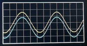
Ah, that's much better. It looks more like the dual-trace capture this really is.
There are more data points and the X axis now accurately represents the LCD's 300 pixels @ 5.1 Ms/s. That's about 59 ms and explains why over two cycles of the 40 kHz input signal are shown.
Refresh
So far, only a single capture is being shown. After that, the code just stops and blinks the on-board LED. Not very practical for actual use.
Here is a continuous capture loop:
refresh.cpp
#include "baseline.h"

int main () {
    baseInit();

    while (true) {
        uint8_t dat [2*GW];
        capture.read(dat, GW);

        for (auto x = 2; x < 2*GW; ++x) {
            uint8_t y = (dat[x] * GH) / 255;
            gfx.pixel({TB+y, TL+x/2}, x & 1 ? TEAL : YELLOW);
        }

        led = 0;
        msWait(100);
        led = 1;

        for (auto x = 2; x < 2*GW; ++x) {
            uint8_t y = (dat[x] * GH) / 255;
            gfx.pixel({TB+y, TL+x/2}, BLACK);
        }
    }
}
It takes a capture, displays it, waits 0.1s, and then clears it again before the next capture. Clearing the trace instead of the entire trace area is far more efficient: drawing 600 pixels to clear the trace vs drawing at least 300x150 pixels.
The LED is turned off while waiting 0.1s to "see" how much time the update takes.
But there are some major problems: the graticule drawn "behind" the traces is gradually being replaced by black pixels wherever the trace was drawn. The other far more disruptive problem is that there is no synchronisation: the traces jump all over the screen.
Such a "scope" display is fun to watch but fairly useless: it really needs a triggered sweep.
Clearing traces
Properly clearing the trace pixels is easy: instead of always writing black pixels, it just needs to write whatever the background was, including the grey pixels used for the graticule. Since the graticule is a simple grid pattern, the pixels colours are easily re-calculated:
Now the background stays intact, because "clearing" knows what used to be there. As before, each update only clears and redraws trace pixels, for a flicker-free refresh.
Triggered sweep
Triggering takes a bit more work. There are a few ways to do this, but for now the approach will be to capture twice the screen area and then look for a transition in the data to find the proper way to place a trace section on the screen. If no transition is found, the screen will still be updated (this is the "normal" trigger mode, "auto-trigger" mode would simply not draw anything until a capture finds a trigger).
This code looks for an upward transition in the middle of the vertical range, and places that in the middle of the horizontal range:
trigger.cpp
#include "baseline.h"
int main () {
baseInit();
while (true) {
uint8_t dat [4*GW];
capture.read(dat, 2*GW);
// locate and align to trigger
auto buf = dat;
for (int x = GW; x < 3*GW; x += 2)
if (dat[x] <= 128-3) {
while (true) {
x += 2;
if (x >= 3*GW)
break;
if (dat[x] >= 128-3) {
buf = dat + x - GW;
break;
}
}
break;
}
// draw the two traces
for (auto x = 2; x < 2*GW; ++x) {
uint8_t y = (buf[x] * GH) / 255;
gfx.pixel({TB+y, TL+x/2}, x & 1 ? TEAL : YELLOW);
}
// restore the graticule
for (auto x = 2; x < 2*GW; ++x) {
uint8_t y = (buf[x] * GH) / 255;
auto c = x/2 % PW == 0 || y % PH == 0 ? GREY : BLACK;
gfx.pixel({TB+y, TL+x/2}, c);
}
}
}
The display is now completely stable (because the signal is a stable sinewave). The 0.1s delay has been removed, but now something else happens: the trace interferes with the LCD display updates. It shows up as a stroboscopic effect: the trace slowly disappears and reappears, since the captures are not synchronised with the LCD's internal scanning.
This is not practical. Trace pixels should not be cleared and restored in separate loops.
Buffered updates
More buffering would help: keep the previous trace until the new capture is ready to be drawn on the screen, then restore the graticule just before drawing each new pixel:
update.cpp
#include "baseline.h"

int main () {
    baseInit();

    uint8_t dat [2][4*GW];             // room for two double-size captures
    auto odat = dat[0], ndat = dat[1]; // old and new captures, respectively
    auto obuf = odat, nbuf = ndat;     // old and new trace trigger starts

    while (true) {
        capture.read(ndat, 2*GW);

        // locate and align to trigger
        nbuf = ndat;
        for (int x = GW; x < 3*GW; x += 2)
            if (ndat[x] <= 128-3) {
                while (true) {
                    x += 2;
                    if (x >= 3*GW)
                        break;
                    if (ndat[x] >= 128-3) {
                        nbuf = ndat + x - GW;
                        break;
                    }
                }
                break;
            }

        // restore the graticule and draw the two traces
        for (auto x = 2; x < 2*GW; ++x) {
            uint8_t oy = (obuf[x] * GH) / 255, ny = (nbuf[x] * GH) / 255;

            if (ny != oy) {
                auto c = x/2 % PW == 0 || oy % PH == 0 ? GREY : BLACK;
                gfx.pixel({TB+oy, TL+x/2}, c);
                gfx.pixel({TB+ny, TL+x/2}, x & 1 ? TEAL : YELLOW);
            }
        }

        // swap old and new buffers
        swap(odat, ndat);
        swap(obuf, nbuf);
    }
}
The code is starting to become a bit more involved, but the buffering requirements remain very modest: 2 traces, each 2x the display width to align to the trigger point, and all of that twice for the current + previous capture. This needs just 2400 bytes of RAM.
One more trick is to avoid redrawing trace pixels which end up in the same place as before. This can considerably increase the update rate for stable repetitve signals such as the current sine wave input, since display updates are currenty the main CPU bottleneck.
There's a subtle bug in the update.cpp code: each trace assumes the display
needs to be restored to the background, but if trace 1 is now on a pixel which
used to be trace 2, then it will be cleared. This never happens here, since
the traces never overlap. To be fixed later ...
A first summary
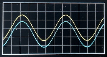
The improvements thus far turn out to be very effective: a stable trigger point for the yellow trace, centred on the LCD, and updating in real time.
With (valid!) single-pixel flimmering as the signal captures from the ADC change ever so slightly.
fps.cpp
#include "baseline.h"

int main () {
    baseInit();

    uint8_t dat [2][4*GW];             // room for two double-size captures
    auto odat = dat[0], ndat = dat[1]; // old and new captures, respectively
    auto obuf = odat, nbuf = ndat;     // old and new trace trigger starts

    cycles::clear();
    auto ms = cycles::millis();
    auto fps = 0;

    while (true) {
        capture.read(ndat, 2*GW);

        // locate and align to trigger
        nbuf = ndat;
        for (int x = GW; x < 3*GW; x += 2)
            if (ndat[x] <= 128-3) {
                while (true) {
                    x += 2;
                    if (x >= 3*GW)
                        break;
                    if (ndat[x] >= 128-3) {
                        nbuf = ndat + x - GW;
                        break;
                    }
                }
                break;
            }

        // restore the graticule and draw the two traces
        for (auto x = 2; x < 2*GW; ++x) {
            uint8_t oy = (obuf[x] * GH) / 255, ny = (nbuf[x] * GH) / 255;

            if (ny != oy) {
                auto c = x/2 % PW == 0 || oy % PH == 0 ? GREY : BLACK;
                gfx.pixel({TB+oy, TL+x/2}, c);
                gfx.pixel({TB+ny, TL+x/2}, x & 1 ? TEAL : YELLOW);
            }
        }

        // keep track and report the display frame rate once a second
        if (cycles::millis() - ms >= 1000) {
            logf("%4d fps", fps);
            fps = 0;
            ms += 1000;
        }
        ++fps;

        // swap old and new buffers
        swap(odat, ndat);
        swap(obuf, nbuf);
    }
}
It's not hard to determine the screen update rate for this signal, using some extra logic:
fps: STM32G431xx @ 170 MHz (v7.0.9-20-g1a79093f)
memory: code 8368  data 32  bss 2460  heap 4  stack 2476  free 27796 b
 138 fps
 166 fps
 150 fps
 150 fps
 143 fps
...
That's still well above the human eye's persistence-of-vision limit. The only visible screen changes are minute signal variations. The G4-Scope screen now looks absolutely rock-solid.
There are now 18 code examples in this project, gradually adding features and improving various aspects of the G4-Scope. It's a long way from being practical with arbitrary input signals, but it also shows that even a "measly" STM32G431 ARM Cortex-M4 µC packs an incredible amount of digital and analog functionality.
All these 18 examples combined take less than 1000 lines of C++17 code. Plus of course the ~ 5000 LOC in JeeH itself. I'm quite happy with these results so far ...
Module build
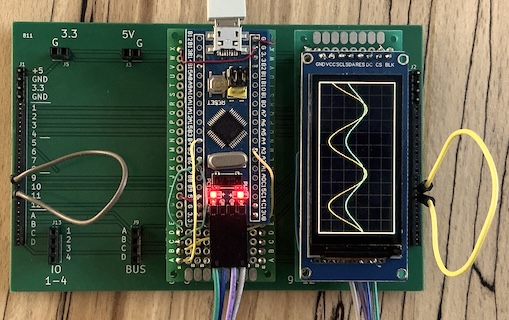
Here is the same circuit as before, rebuilt on a 7x3 cm proto board:
ADC1 and ADC2 are connected to IO-1 and IO-2, which makes them available on
the right and left headers. The DAC signal output is on IO-3. The jumpers
connect the DAC to the two ADCs, to provide the sine wave shown on the display.
The board in the middle is a BluePill, configured as Black Magic Probe. It powers everything over USB, and enables both uploading and viewing log output over RTT.
Adding a LIN bus
The LIN bus will be used to control this scope with some real knobs – knobs are nice! – the tactile feel will be more effective than a touch panel on such a tiny screen could ever be.
Two new modules should make this a workable option: the LIN Monitor which orchestrates and displays all LIN bus activity, and the Rotary module with some knobs and buttons:
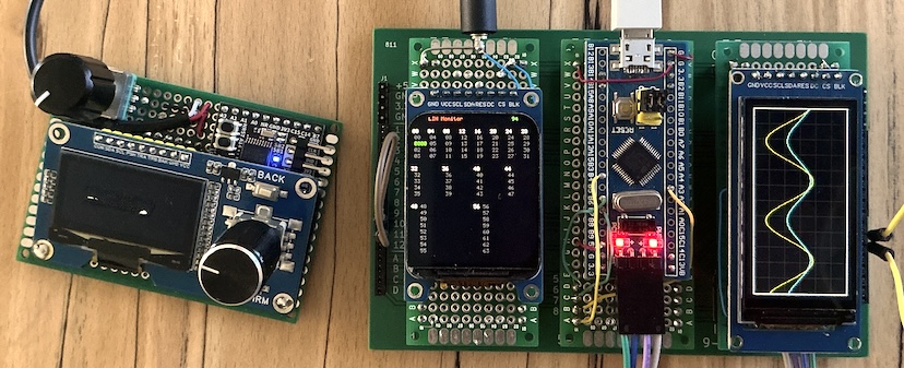
The rotary module is connected via a 3-wire 2.5mm "TRS" plug. All it needs is power and the LIN bus signal line. A short cable makes it easier to place it in a convenient spot.
Turning knobs and pushing buttons shows up as changes to packet ID 1 (the green text in the top left). All the scope has to do now, is listen on the bus and pick up these packets.
Ehm ... it's far more involved than that: how do you change the timescale of the scope's ADC captures? How do you move traces up and down, or change the trigger point? Even more involved: how do you change the ADC's voltage ranges, i.e. the scope's sensitivity? Or, ehm ... calibrate all this, at least well enough to make those scope traces meaningful? Speaking of which: the current scope settings will also need to be shown somewhere.
Signal sensitivity (and Nyquist low-pass filtering) are analog issues. These will have to wait. The first challenge is to implement manual control of some settings ... and applying them.
Background LIN
JeeH includes a "LIN task" to deal with LIN in the background. Here is a basic example:
lin.cpp
#include <jee.h>
#include <jee/hal.h>
#include <jee/util/lin.h>
using namespace jeeh;
#include "defs.hpp"

Ticker ticker;
TICKER_TRIGGER(ticker)

util::Lin linTask (linBus);

uint8_t* util::LinPoll (uint8_t) { return nullptr; } // not used

void util::LinRecv (const uint8_t* ptr, int len) {
    if (*ptr % 64 == 1)
        logDump(ptr, len);
}

int main () {
    initBoard();
    linBus.init(19'200);

    // init all tasks in decreasing priority
    linTask.init();

    while (true)
        asm ("wfi");
}
It obviously also needs a UART, which has to be set up in non-blocking mode
(uart::Trig) and with its associated interrupt handlers properly defined in
defs.hpp:
... as well as a matching line in platformio.ini to select the proper UART and
pins:
This uses the G431's USART1, with pin B6 as LIN bus pin (open-drain + alt mode 7).
Note
This sort of setup is not trivial: it depends on many pesky little details, since the UART is used with DMA and asynchronously from a backgrund task. It takes some sleuthing and getting used to, but all these details can be found in G431's "RM0440" reference manual, sections "USART" and "DMAMUX".
Sample output:
lin: STM32G431xx @ 170 MHz (v7.1.0-18-g8f4eb421)
 000: C10000                              ...
 000: C10200                              ...
 000: C10500                              ...
 000: C10500                              ...
 000: C1053F                              ..?
...
One knob was turned clockwise (0 -> 2 -> 5), the other counter-clockwise (0 -> 3F). Polling is only once every 500 ms, else many more packets would be received in rapid succession.
This example merely logs LIN packet reception for ID 1. It can easily be adapted further.
Trace math
Getting a "proper" trace on the screen is more complicated than I thought ...
One issue is that ADC acquisitions do not happen on exact grid points: the ADC clock has its own µC-based rate, whereas the screen needs to show a trace on a 1-2-5 step µs or ms per division X-axis. The same holds for the Y-axis: the ADC is set up to sample only 8 bits (for top speed), but the screen shows 6 divisions of 25 pixels, so the samples will not be exactly on a grid point in the vertical direction either. This all requires some sort of interpolation.
But that's the easy part. How do you show a trace of say a 500 kHz sine wave when the ADC is sampling at 5 Msps? Each cycle will have 10 samples. What if you want to zoom in and show one cycle on a horizontal scale of say 10 divisions, i.e. 250 pixels? That's 200 ns/div, i.e. one sample per division: arguably beyond the limit of what a 5 Msps scope could show, but it's still enough to distinguish sines from square or triangle waves, for example.
The lazy answer is: use linear interpolation, i.e. draw straight lines between each point. Unfortunately, the result looks awful: even a clean sine wave ends up as a stick drawing.
There is a better solution: sin(x)/x interpolation, which is what all "real" oscilloscopes use. But this requires some serious DSP code plus some math, and is worth its own article. It's an almost magical technique which hinges on having a good anti-aliasing filter in the analog front end (as required anyway for all discrete, i.e. ADC-based, sampling).
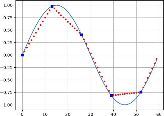
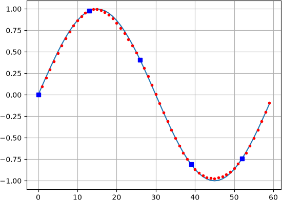
On the left: linear interpolation. On the right: sinc + Lanczos interpolation. I rest my case.